


Cleaning & Disinfection, Knowledge Base
Particles on Surfaces: Part 8 – How Clean is Clean For Microelectronic Companies?
Feb
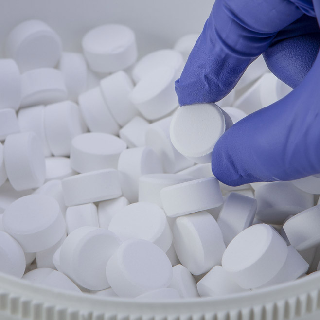
Let’s focus on one of the most challenging cleaning requirements for the pharmaceutical industry – cleaning equipment used to manufacture injectable materials – so called “parenteral drugs”. These materials must be made in environments that are absolutely clean and sterile, because there is no opportunity for the drugs to be sterilized after packaging – i.e. no possibility of “terminal sterilization”. Not only that, but after a manufactured lot is completed, the equipment and the room housing it must be cleaned so that no traces of either the manufactured drug or the cleaning agents are left on the surfaces… and you thought keeping a clean kitchen was difficult!
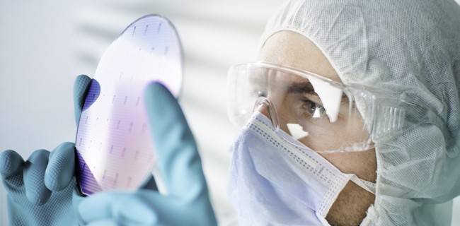
The largest silicon wafers in use today measure 300 mm (approximately 12”) in diameter – roughly the size of a dinner plate. Wafers this size are extremely pure and can be made extraordinarily clean, with only a few particles residing on the wafer. The value of bare silicon wafers (also known as “prime” wafers) increases by orders of magnitude when the IC circuitry is incorporated into the wafers. The need to protect these wafers from particle contamination is paramount, since even submicron-sized particles (those with diameters well below 1µm) can ruin the complex circuitry on the wafer. The procedures described below for surface cleanliness verification were developed to ensure the extremely high value of the finished wafers and to guarantee that defects are absolutely minimized.
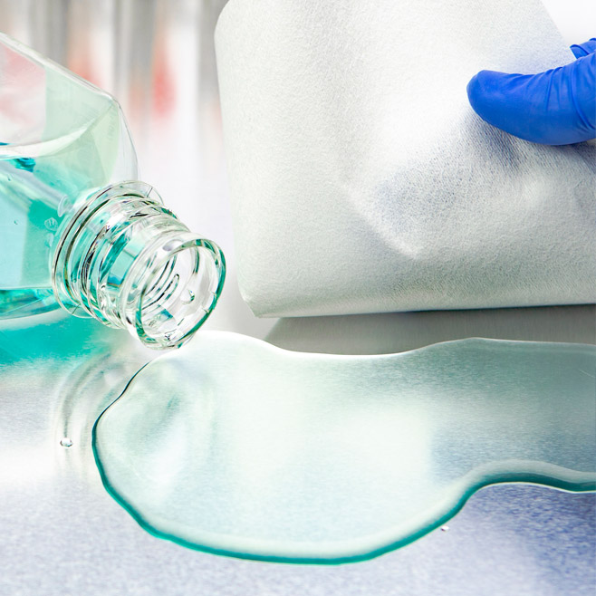
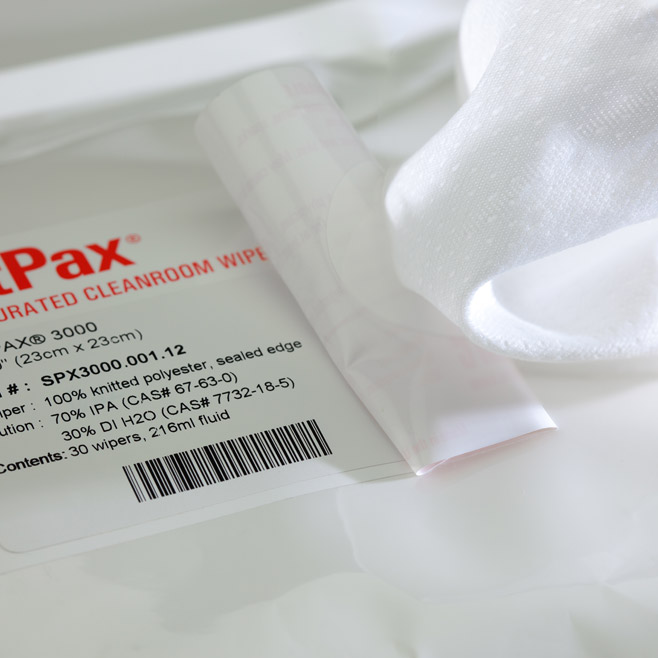
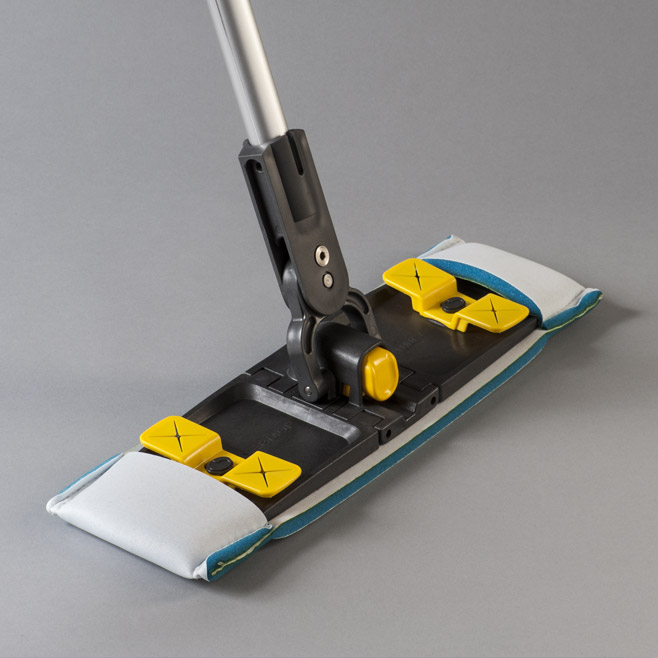
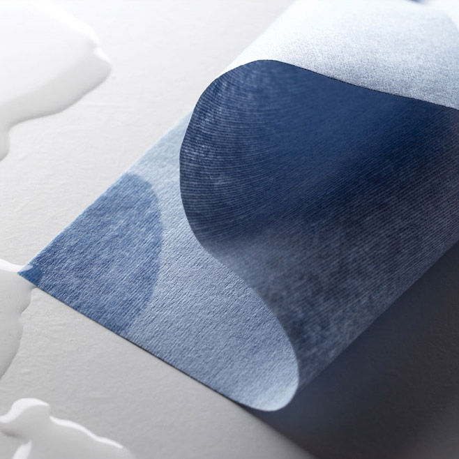
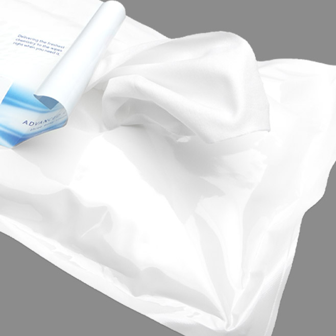
The manufacture of ICs involves hundreds of sequential steps in which thin films are deposited, etched, patterned and smoothed to ultimately form memory chips, controllers, logic circuits, etc. This is accomplished in a variety of sophisticated, robotically-controlled process tools. Periodically, this equipment must be cleaned using physical and chemical treatments and where appropriate, very clean, ultra-low ion, polyester knit wipers. These treatments remove the process residues and particles which otherwise might ruin future wafers. Given the extraordinary value of the wafers as they move through the process cycle, the need to remove residues and accompanying particles is cardinal.
Finally, we have arrived at the nub of the issue. How do the IC manufacturers know that the equipment has been cleaned sufficiently and that particle levels within the cleaned equipment are at acceptable levels?
Fortunately, they can rely on a well-established property of particles on surfaces – i.e. particles will scatter light impinging on them. If you can detect and measure the scattered light, you can identify the presence of particles. To capitalize on this, a logical and clever procedure for assessing particle levels in process equipment has been developed.
A prime wafer (with no circuitry on it) is placed into a computer-controlled, laser-scanning instrument to record a particle map of the entire wafer surface. Any particles on the prime wafer will scatter the laser beam and show up on the wafer map as dots. The instrument automatically counts and records the number of dots on the prime wafer. As mentioned above, prime wafers have very few particle counts, so this establishes a low baseline for the next measurement.
The prime wafer is then passed through the process equipment that has been cleaned. No processing is done on this wafer – the sole objective is to cycle the wafer through the equipment to have the wafer collect any particles that impinge on it (mimicking what would happen if a wafer containing ICs were passed through the equipment) . The wafer is then measured again in the laser-scanning instrument and the particles again counted and recorded. The net increase in particle counts from the two measurements on the prime wafer represents the particles contributed by the equipment during the cycling activity – the so-called particle “adders”. If the adders are within acceptable limits, the equipment can be returned to the line for processing more wafers. If not, the equipment must be re-cleaned. The cost of the prime wafers for these measurements is negligible compared with the value of future finished wafers incorporating ICs.
The reader will note that the methodology developed by the semiconductor industry for verifying surface cleanliness is totally different from the methodology used by aseptic pharmaceutical manufacturers. Each industry uses the approach that serves its needs best.
In this series of articles, we have covered topics such as the deposition of particles on surfaces, the binding forces that hold particles to surfaces, the optimum methods for removing particles from surfaces using wipers and mops, and finally, the verification of surface cleanliness.
You can download this complete series in PDF format by completing the form below

HAVE AN IDEA FOR CONTENT?
We are always looking for ideas and topics to write about.
Contact Us